
About ChinaPCB
PCB and PCBA factories in China, checked one by one. The purpose is narrow: a buyer should be able to find the factory that can actually build their board, read what that factory can prove, and then deal with it directly.
Who runs ChinaPCB.org
ChinaPCB.org is operated by Weis Technology Co., Ltd., a company based in Shenzhen, Guangdong, China. It is an editorial directory and is not affiliated with any manufacturer listed here.
| Operating entity | Weis Technology Co., Ltd. |
|---|---|
| Registered address | Room 398 Guanlan Avenue, Guancheng Community, Guanhu Street, Longhua, Shenzhen, Guangdong, China |
| Editorial contact | [email protected] |
| Coverage | Mainland China PCB and PCBA factories |
| Commercial relationship | Editorial directory; not affiliated with any listed manufacturer. A profile is an editorial record, not an endorsement. |
Because the domain contains a country name and uses a .org suffix, we publish the operating entity, its registered address, the editorial method and the correction channel in the open. Where a fact could not be checked against a primary source, we leave it visibly unconfirmed rather than fill it with an estimate.
How a profile is put together
One page per legal entity, with capability recorded per product series. Layer count, base material, surface finish, certification and MOQ are the fields a profile is built to answer, and every factual claim carries an evidence level and the date it was last checked. A marketing maximum published for one product series is never carried over to another, and a group parent is never merged with the subsidiary that runs the line.
What this site does not do
It does not run an RFQ auction, does not sell enquiry leads, and does not sit between a buyer and a supplier. There is no agent in between and no request form that goes nowhere. Read a profile, contact the factory on your own terms, and write to [email protected] only if you want to reach us.
Listings are not for sale. A factory cannot buy a better evidence level, and no ranking on this site is sponsored.
About the photographs
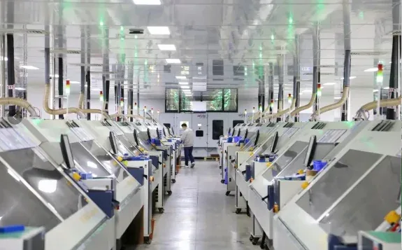
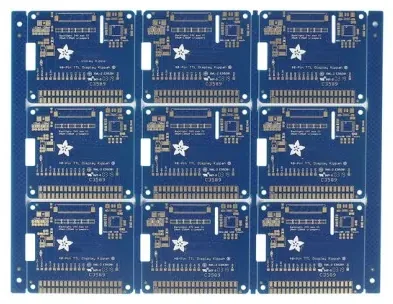
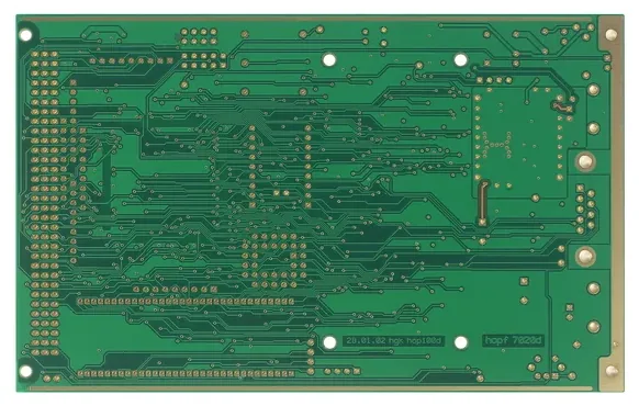
The photographs on this site are real production photographs of PCB fabrication and assembly. They are used to show what the processes look like, not to picture the plant of any particular listing, and a factory profile is never illustrated with another company's plant. Photo credits are recorded in /images/CREDITS.txt.
Contact and corrections
Email [email protected] or write to Weis Technology Co., Ltd., Room 398 Guanlan Avenue, Guancheng Community, Guanhu Street, Longhua, Shenzhen, Guangdong, China. For a correction, include the profile URL, the field you believe is wrong and a primary source that supports the change. We record the change and update the review date on the profile. See how we verify for the evidence levels we use.